Return to home page
I have built such an amplifier for a friend whose Newport meter broke down but who has some detectors plus their calibration data sheets. In fact essentially all what these fancy meters do is to amplify the detector current and display it, after taking the stored calibration data into account. This can also be easily done with a simple transimpedance amplifier and a DMM, if one is willing to multiply the result by the calibration factor by hand.
The 818 detector datasheets have four lists of data, and each list gives the wavelength dependent cal data for every 10nm over a given range. The first two lists are the responsitivities (mA/mW) for the bare detector, and for the detector with attenuator (which reduces by a factor of approx 1000). The last two lists are the inverses of these, ie, display mW/mA. So all what one needs is to measure the current through a detector and multiply by the relevant mW/mA factor.
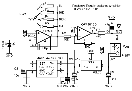
Since one needs to measure the current as accurately as possible, the best thing is to use a transimpedance amplifier that converts current to voltage in a suitable range, which has also the benefit to have (almost) zero input impedance which is important for linearity. A transimpedance amplifier is extremely simple, essentially it consists only of an opamp plus one resistor R, whose value determines the conversion factor according Ohms law: Uout = Iin R. So it is almost not worth to describe it, on the other hand I realized that some things may not be obvious for people without electronics experience. Moreover there is always a gap between the abstract idea for a circuit and an actually working circuit which has been optimally designed and tried for a given purpose. So that's why I mention the circuit here, its schematics are as follows:

IC2A is the actual transimpedance amplifier, whose conversion factor can be switched by three or four orders of magnitude. IC2B inverts the signal to be positive. IC2 = OPA1013 is a high precision, low noise and low offset dual opamp. It requires a negative supply voltage for reaching zero volts output, and this is generated by a MAX1044/ICL7660 charge pump. Overall, the supply is reduced to 5V by a voltage regulator, that total current draw is like 3mA. R7 helps to protect a possible ADC and also forms together with C4 a low pass that cuts down 50Hz ripple. D2 protects C4 and a possible external ADC from negative voltage spikes.
For high accuracy, all resistors except R7 should have a precision of 1% or better; I hand-selected the resistors to around 0.1%. I checked the circuit to be very linear over the full range; the noise is less than 1mV at highest gain (~1nA) , the offset 7mV at highest gain (~7nA bias offset), the max saturation voltage out is approx 4.5V (it could be increased to 10V and more by having the positive voltage pin of IC2 connected to the supply voltage, but I kept it at 5V in oder not to endanger external ADCs which often have a limit at 5V or so).
The top range with R=1K yields 1V/mA, so this captures well the max power of the 818-SL sensors with attenuator, which is 2W giving around 1mA. For the 818-X-UV sensors the max power is 0.2W~ 100uA, so the second setting with R=10K and gain 10V/mA is appropriate. The other settings are useful for low intensity measurements, and if the attenuator is taken off, they can be used for holograhic exposure measurements as well. Alltogether 7 orders of magnitude of power can be spanned this way. For R=1M the max. gain is 1V/uA, which then yields a max. sensitivity of order 1V/uW, which gives nanowatt resolution.
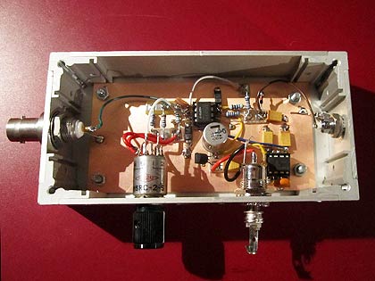
For measuring small currents, a proper layout including good shielding is important:

Vers 1 12/2010