Return to home page
This is an interesting, though not too powerful optically pumped semiconductor laser (OPSL). The board looked new but the head was used and sold as "probably not up to specs". The internal Eprom had listed some 4000h operating hours. Indeed so, I measured 9.6mW instead of 20mW, but at least flawless single longitudinal mode. However I was playing with the computer interface, and found that the internally measured power was 20mW ... so the controller believed the laser was up to full power. It seemed that somehow the monitor diode got misaligned or so; certainly I checked the output window whether there could be some back reflection, but it was mint. That made me wonder whether one could trick the controller by reducing the feedback signal in order to compensate for the "excess" power. This indeed worked out but it required a certain degree of reverse engineering. Before I explain this, I like to first describe the system as a whole.
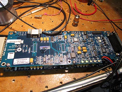
The system consists of a controller and a separate laser head, linked by a standard DB25 cable. The controller is microprocessor based and allows to enter and recall various system parameters via a standard RS232 interface, like power, diode current, diode temperature, etc. Somewhat surprising is the amount of effort, the controller consists of two large densely populated PCBs. The upper contains the digital processor while the lower hosts various nested switchmode regulators. On wonders what is really necessary beyond a simple LD and TEC driver....At any rate, it offers numerous safety features. I think it is pretty hopeless to figure out the various jumper and analog interfacing options without the manual.
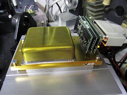
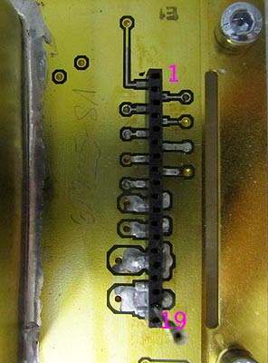
The laser head is quite compact, and my initial hopes to have it easily fixed were dashed when I opened the outer case: all what was revealed were 3 stacked small PCBs, and the very laser head turned out the be hard-sealed and there seemed little point to try to open it without damage. So first thing was to figure out the connections between the PCBs and the head. For this I put some prolongation pins on the interface connector, in order to measure voltages and waveforms:
In this way, the following pinout was determined (plug 19pin 2mm grid):
 |
|
Probably one can run the head by simply connecting a temperature controller and diode driver. For this it may be helpful to note some values I found: LD temp 20C; thermistors are standard type 10K at 25C; LD current limit 1.8A (this is seen when opening the photodiode loop). The four unknown connectors A,B have pairwise a resistance of approx 100 Ohms and get full supply voltage at startup, which then goes smoothly down to like 5.6V; these may or may not relate to some thermal control of other components inside, like of the laser and SHG crystals; hard to tell without opening.
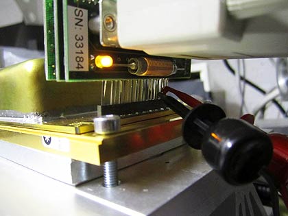
Surprising is also the amount of circuitry on the three small boards; the first, outmost one mainly houses the connectors; the middle one contains an AC amplifier (it sports high bandwidth opamps plus power RF transistors). Apparently this is used to provide a high-bandwidth feedback loop for reducing noise. It also has three trimpots, one of which is accessible through a hole in the case which is hidden below the label. This sets the AC gain, and adjusting it randomly make the whole amplifier oscillate with many volts output on the laser diode! The latter must have a good protection inside the laser case, otherwise it would have been destroyed from this. The other two pots provide symmetric biasing of the AC amp and set the drive to the power stage, resp. I guess there is no need to ever play with them. Moreover, at the side there is also a little 2-prong jumper plug, which is also accessible through another hidden hole from outside. Jumpering it seems to bypass the feedback loop, which is probably used for tuning the system.
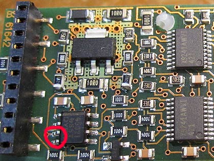
The third, innermost board contains a DC feedback amp, two multiple non-volatile digital pots for storing setpoints, and some other DC stuff. This is where we do our little modification. All what is necessary to reduce the input signal from the photodiode appropriately, by placing a resistor between the non-inverting input and negative ground of the TLC4502 input opamp. I found that for R=1.2Meg the internally measured output matches well the actual output at 20mW (this is nonlinear and indicates eg 5mW for actual 6mW). The value needs to be tried out, just note that there is a 1Meg series resistor before and we can think of the extra resistor as acting as a voltage divider against this 1Meg. See the location on the following pic (the resistor is not visible, I placed it on the backside):
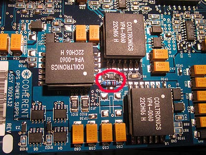
Moreover, I noticed that the 20mW output was just barely reached due to the current limit of approx. 1.8A. In order to have some margin if the laser efficiency drops further, I also modified the sense resistor of the LD current limiter. It is located on the lower PCB of the driver, see the pic below. The sense resistor is 0.015Ohms, and I added an extra 0.2 Ohm parallel,so this gives 7.5% additional max current, which seems within safe limits (probably the diode can do 2A).
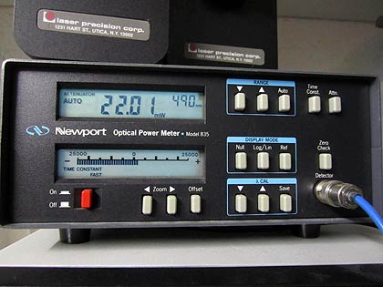
After these modifications, the laser happily runs more than 20mW:
.. and displays nice stable single-longitudinal mode operation over practically all of the power range (checked with the scanning interferometer):
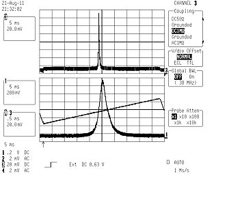
The lower trace is a 10-fold zoom of upper trace, ie, approx 20Mhz/Div. The line width thus is in the order of at most 20Mhz, and so the coherence length at least several dozens of meters!
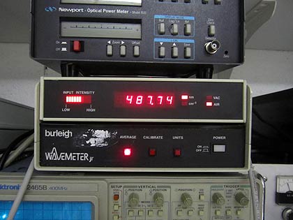
The output is close to the 488nm Argon line:
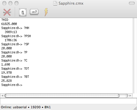
All seems fine:
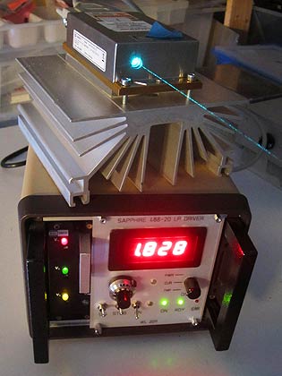
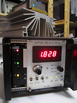
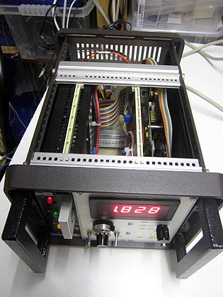
Finally I put the driver in a case, with various analog and digital controls, and voila, a nice sweet system ready for holography:
Vers 1.0 09/2011