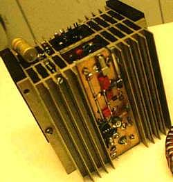
This unit is entirely on the heat sink, the drive signal and the power out signal fed by shielded cables. In particular the MC33152P Mosfet driver IC is close (~1-2cm) to the gate pins of the two power Mosfets. This gives a rise time from 0 to ca 12V of the order of 30ns on the gates. Note that this IC is rated at 85C max, so one needs to make sure that the sinks don't get hotter than this. The diode is on the sink on the back, connected to the mosfet drains by a 1cm wide copper strip running straight in the middle between the sinks. The sinks are larger than necessary, but I had them in the case anyway and this certainly doesn't harm; at 12A per power unit they just get lukewarm.
The IRF460 mosfet source leads are as short as possible, like ca 5mm in total; to ensure this, I placed a one-sided copper clad epoxy board on the "other" side of the sink (opposite to where the TO-3 cases stick out), the copper surface forming the ground to which the source legs are soldered. The gate pin and screws for the drain connections stick through isolated holes of this board. The drain-connected TO-3 cases are insulated via mica washers from the heat sink (to reduce EM radiation noise).
The free-wheeling diode dissipates energy at the same order of magnitude as the mosfets, so a diode with high current margin and good cooling is necessary; I finally chose a hyper-fast soft recovery diode (trr=40ns) RHRP3060, which can do Icont=30A and Ptot=125W (the well-known MUR1560 (15A) may do as well but doesn't have a large safety margin). Other diodes such as MUR3080 (30A) switch slower and run significantly hotter. All connections around the diode are as short as possible, as are the legs of the snubber RC-combinations and Zener protection diodes. The diode may be put on its own heat sink connected to the "+" power feed. A very good capacitive blocking between the "+" power feed and the Mosfet source ground is crucial to avoid excessive ringing; I have put a 1uF MKP 400V cap here (in series with a 1 Ohm damping resistor, which makes a huge difference !) plus smaller FKP type ones. After optimizing snubbers etc, I found very little voltage overshoot at the drains and no overshoot at all at the gates, at full power. This allows me to use the 500V Mosfets I happened to get (IRF460 I/P=21A/300W) directly off the AC line (310V after rectification). However, due to lead inductance the negative voltage undershoot directly at the diode body is larger.
The drive signal is fed through a thin coaxial cable from the isolation unit b), as is the 15V feed for the IC. The output cable coming from the Mosfet drains is also shielded, the shield connected to the "+" power feed at the diode heat sink; it can be at least 20-30cm long without making problems. Due to the high current the cable needs to be relatively thick, unlike the usual coaxial cables. What I did was to put a copper mesh sleeve around an ordinary installation wire, and isolated the whole thing by a shrink tube on top of that.
Note that several "power units" units can be used in parallel, I use two units in order to safely drive my 25A Coherent and Lexel heads; a single unit is adequate for the ubiquitous 100V/10A argon laser heads. Each of these power units connects to its own inductor in the Filter unit .
Variations of this setup are possible, but I wouldn't directly connect more than 2 mosfets in parallel; otherwise the diode will become the bottleneck (and perhaps the inductor as well), and diodes are not easy to use in parallel. A better variant would be to use one cheap MUR1560 diode and one lightweight inductor per mosfet (each with an individual driver), and use a larger number of mosfets. More modern would probably be to use just one hefty IGBT module, but I don't have any experiences with that. At any rate, the current capacity of the semi-conductors should be at least double or triple of what the laser needs, in order to have some safety margin.
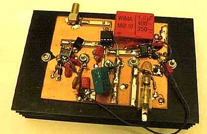
This is a test version which worked equally well, the diode is in between the mosfets; this gives longer connections and so I had used a driver IC separately for each mosfet.
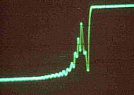
The tricky part of the whole circuit is to ensure shortest switching times while keeping the mosfets and the diode within safe limits (short switching times are necessary for having low power dissipation). Short switching times however also mean voltage spikes induced by the rapid change of drain-source voltage and current. Generally the spikes grow with the inducance of the wires, which means that all wires around the mosfets and the diode must be as short as possible (a few millimeters, preferably). There are several kinds of potential problems:
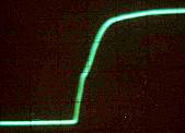
It is important to try out a circuit at low voltage, say 30V, and slowly tune up the current and monitor how waveforms at drains and gates (and through the inductor) behave. Make sure you understand exactly what is going on and that everything looks ok, before you raise the voltage to 150V and finally, 310V.
If the voltage spikes cannot be well controlled (eg due to long leads), or if one wants to cut down on radio interference, one may increase the switching times at the expense of power dissipation. This can be done by adding (short-leaded) resistors in series with the gates (the protection diodes stay at the mosfet side, of course). Such resistors may be a few til a few dozens of Ohms. Be careful to make them not too large, as the induced gate voltage variation will be less suppressed.
The power dissipation is very low; for moderate switching frequencies it comes mainly from the finite "on"-resistance Rds of the mosfets. In order to give some feeling for this, I have plotted the Ptot per mosfet as a function of total output current, first for 2 and then for 4 Mosfets IRF460 in total. The other data are: f=80khz, Vin=310V, Vout=100V, (on+off) switching time=100ns, Rds=.3 Ohm. Each plot shows two curves, the lower one is switching losses only, the upper one is the total Ptot including the "on"-resistance. You see that the power dissipation is quite moderate.
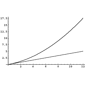
Ptot (W) per mosfet depending on output current (A), with two IRF460 in total
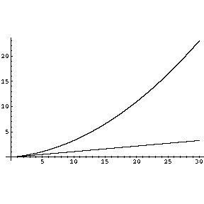
Ptot (W) per mosfet depending on output current (A), with four IRF460 in total