Return to home page
The controller also figures as central part of my newly revamped test system for laser diodes, which does automated linewidth/mode scans over diode current/temperature to identify good operating spots with single mode operation. The system includes also an extra analog front-end for conditioning the signal from my CCD spectrum analyzer, and a laptop. See the movie for the complete setup:
The blue trace on the scope is a measure of the relative line width - see how it goes up as the number of modes increases, and vice versa. This allows to automatically generate landscape plots of the mode structure as function of diode current and temperature.
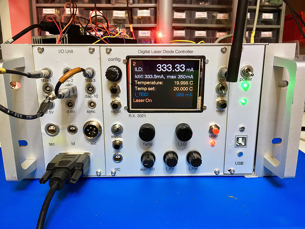
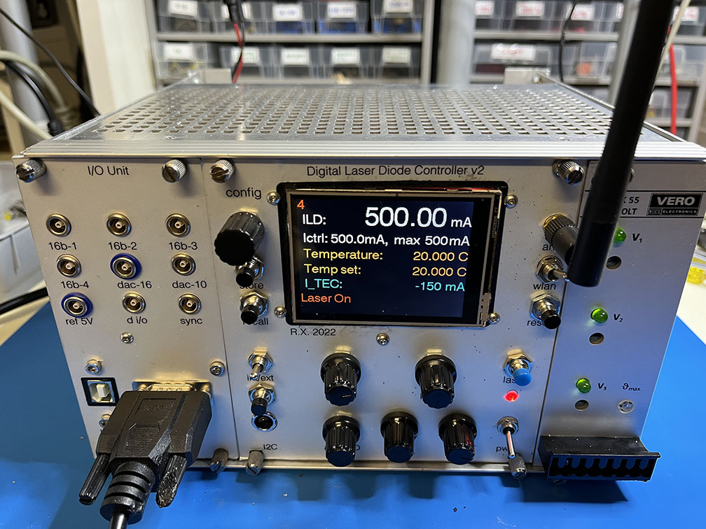
Precision digital laser diode driver
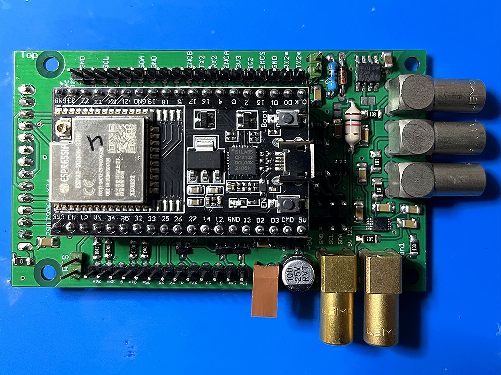
Display, WLAN and IO driver board
Related: Some remarks on a LT3045-based linear regulator
Finally I managed to complete a project of many years, a highly stable digital laser diode control and data acquisition system. The Arduino based TEC controller back in 2017 was a first step, and now I added a digital diode driver and a TFT display unit and WLAN interface, and put all together. This is spiced up with some data acquisition features including full remote digital control. This is for tasks like automated scanning over diode current and temperature to find the best (single mode) operating spots, via LabVIEW running on an external computer. WLAN allows to avoid noisy data and ground connections to a computer. Digital control also makes it easy to use rotary encoders for manual operation, to order to avoid potentiometers which have notoriously bad temperature coefficients (talk about 100ppm/C). In this way one can map all relevant quantities to a stable voltage reference and low tempco precision resistors.
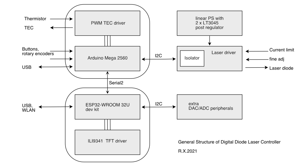
In the meantime, better microprocessor boards than the Arduino became popular, notably ones based on the ESP32. However, I didn't want to redo my work for the Arduino-based TEC controller, since that is really very much optimized for the Arduino and thus would be cumbersome to port. So I decided to keep the Arduino, albeit in its Mega 2560 variant which has more IO ports and more memory. TFT and WLAN interfacing was relegated to a separate board based on the ESP32. The laser diode driver is accessed via an isolated I2C bus. A key feature is that the laser diode driver is galvanically completely isolated, except for one single connection to system ground. This, in conjunction with a dedicated floating linear power supply with low noise regulator, helps to achieve minimal noise in the otherwise heavily digitally polluted environment.
The Arduino is interfaced via serial bus to an ESP32 dev board which figures as TFT display driver and WLAN frontend. It supports also via a separate I2C port a number of extra data acquisition components. Separating the interface circuitry from the Arduino Mega avoids interference with the very intricate timing setup of the PWM controller, and also makes the wiring easier. As it turned out, operating the two microcontrollers in tandem works well and was less cumbersome to set up than I had anticipated.
Here is a sketchy overview of the setup:
There are various operation modes, either fully with internal TEC and LD drivers, or for mixed configurations with external components, also there is a dedicated PL530 mode for dealing with the Osram PL530 OPSL.
Here are some key features of the various functional components:
1) Diode current controller:
-delivers up to 512mA
-noise approx 0.3uA/pp for 0.1-10Hz, at 400mA
-voltage compliance about 7.5V at 500mA, could be improved by raising supply voltage
-<2ppm/C voltage reference and 2.5ppm/C current shunt resistor
-fully 16 bit DAC digitally programmable output (approx 8uA resolution),
with 16 bit ADC readback to monitor actual current, controlled via I2C bus
-12 bit ADC readback of setpoint, available before laser is on
-12 bit ADC readback of current limit, settable manually only per pot for safety
-external pot for continuous fine regulation, spanning about 1mA
-monitor of output voltage to determine short or open diode to initiate shutdown
-complete galvanic isolation from rest of the instrument, except for a single ground connection
-buffered export of 5V reference voltage and DAC output for external applications
-dedicated ultra low-noise linear power supply based on LT3045; for some observations see here.
For more details, see below.
2) TEC PWM controller
- full PWM H-bridge for bi-directional TEC drive
- up to +/-3A current in intervals, +/-2A continuously
- configurable current limit
- standard 10k Thermistor for sensing
- setpoint range about 10 degrees
- temperature stability ~ 1/1000 degree for extended periods of time
- noise level about 2/10.000 degrees
- PWM ripple about 5mV/pp at 50:50 duty cycle (improved)
- auto turnoff for open/shorted thermistor, temperature out of range, and H-bridge overtemp.
- automatic PID control loop configuration per pushbutton, saving data to EEPROM
For more details, see here.
-runs most of the software: for the TEC PWM controller as attachable shield, and for the diode driver via I2C bus
-serves rotary encoders for TEC temperature and diode current
-serves most front panel buttons
-interfaces via Serial2 bus to the ESP32 IO interface
-saving and recalling configuration settings to/from profiles, including diode current, temperature and PID regulator data
4) ESP32 interface board for display, WLAN and IO driver
-attaches directly to an ILI9341 based standard 2.8'' TFT board
-ESP32-WROOM-32U dev board attaches on top
-serves Arduino Mega via Serial-2 port
-serves ADS1115 4-channel 16 bit DAC via I2C
-5V level shifters for Serial2 port to Arduino and I2C
-some digital/analog IO lines, 3.3V/ 5V
-WLAN support via external antenna
For little more details, see here.
5) Extra analog/digital IO board
-delivers high precision (12 and16bit) analog input and outputs, intended for making measurements for lasers with their own driver boards.
-sits directly behind the front panel to minimize wire paths and interference.
For more details, see here.
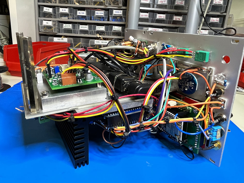
At present the whole unit looks like that, but I plan to improve on the shielding in the future:
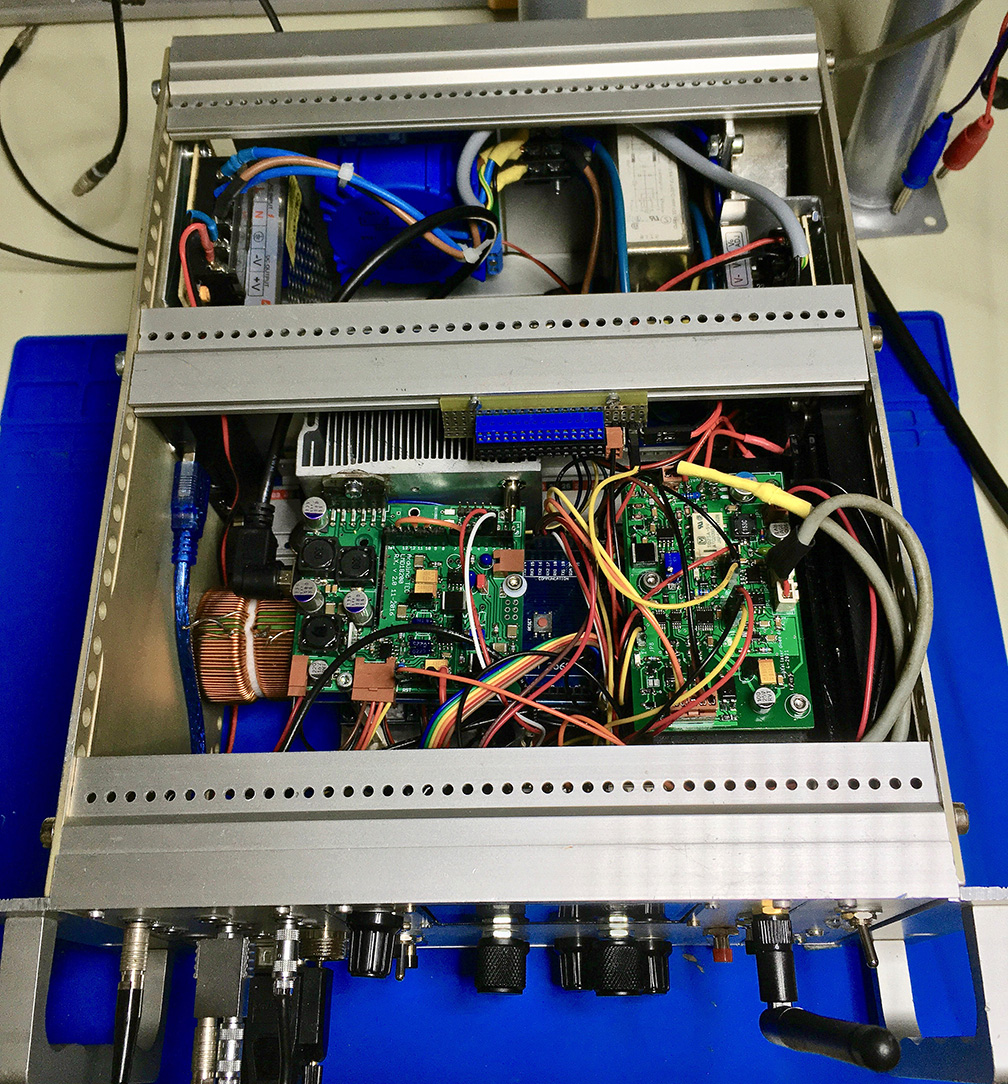
Always underestimated: the cabling of the components, incl the controls and IO ports at the front panel. For sure the dullest part of all, but the most enerving, even with wire-reducing design it got out of control. Without taking pictures and logging all connections in a file it would be virtually impossible to repair/reassemble in the future.
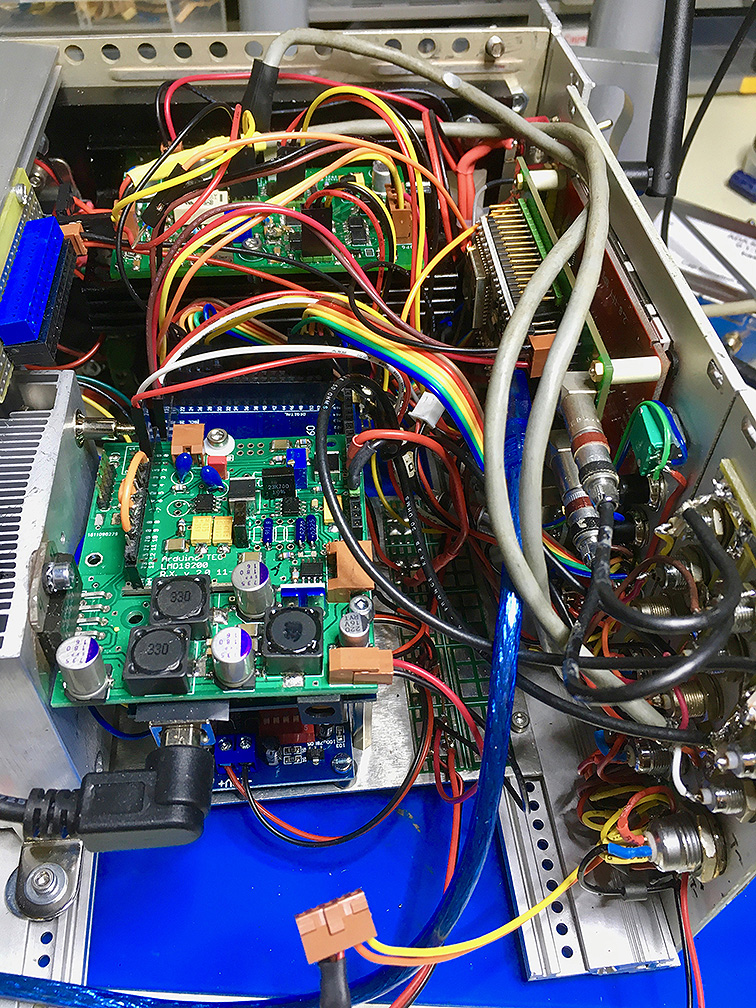
Update 12-2022: Since I had enough spare parts left over from the development work, I decided to build a second version. Since it uses an older version of the diode driver board and does not use an extra linear power supply for it, nor has a high precision IO board, its specs are not quite as good, but that is less important for a backup unit. At least I mounted all parts together on one slide-in tray facilitated the cabling and maintenance.
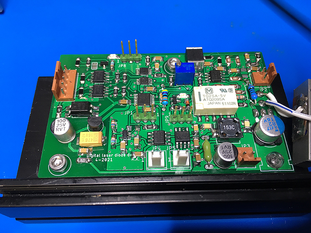
Precision digital laser diode driver
-delivers up to 512mA
-noise approx 0.3uA/pp for 0.1-10Hz, at 400mA
-voltage compliance about 7.5V at 500mA, could be improved by raising supply voltage
-<2ppm/C voltage reference and 2.5ppm/C current shunt resistor
-fully 16 bit DAC digitally programmable output (approx 8uA resolution),
with 16 bit ADC readback to monitor actual current, controlled via I2C bus
-12 bit ADC readback of setpoint, available before laser is on
-12 bit ADC readback of current limit, settable manually only per pot for safety
-external pot for continuous fine regulation, spanning about 1mA
-monitor of output voltage to determine short or open diode to initiate shutdown
-complete galvanic isolation from rest of the instrument, except for a single ground connection
-buffered export of 5V reference voltage and DAC output for external applications
-dedicated ultra low-noise linear power supply based on LT3045; for some observations see here.
Here are the schematics:

Remarks:
I didn't attempt to keep it as simple as possible, rather I tried to make it as good as possible with reasonably easy obtainable parts. A main feature is the full galvanic isolation in order to fight coupling of digital noise from the microprocessors, and above all, the PWM TEC controller. The isolation part is to the left of the schematics, where there are two ISO1540 bi-directional isolators for the I2C bus. Their left-hand sides talk to the outside world. There is a dedicated isolator to control the MAX5217 DAC, whose output drives the laser current controller; its connection to the I2C bus is made only briefly when the DAC output is to be changed. This is for eliminating bus feedthrough noise on the output, and is controlled by an extra trigger signal via the opto coupler OK1.
The actual diode current on/off is achieved by a - gasp- old fashioned relay, K1 (to avoid misunderstanding: this is on the input side of an opamp, rather than acting directly on output). Past the relay, the low pass R10/C7 provides a soft start-up. The main reason for a relay is that mosfet switches typically will have a minute, temperature dependent current leakage when off, upsetting the input bias currents to the OP213; we are talking about really very small currents here. A relay provides robust temperature stability and complete galvanic isolation, and the second pair of contacts provides, as a by-product, a resistive clamping of the laser diode when off. This in turn allows a soft discharge of possible filtering capacitors further down the line.
There are two ADC's controlled by the other I2C isolator ISO1540, namely the 16bit MAX1169 for monitoring the actual diode current, and the 12 bit, 4 channel MAX1236 for monitoring, first of all, the laser current set point - independently from the output being on or off. This means that one can check what the current would be before actually turning on the laser diode. This is especially important when recalling a stored operating setpoint: you might have forgotten that the stored setpoint exceeds the allowed rating of that new expensive diode. It also prevents, per software, turning the current setpoint beyond the chosen limit. The current limit in turn is set by an external potentiometer, which is read by another channel of the MAX1236. There is no way to change the current limit other than manually turning the pot, which is an important protection feature for the diode. The third channel of the MAX1236 monitors the output voltage across the diode, which allows to recognize shorted and open diode connections. In such a case the current quickly turns off. This is a protection against bad contacts in the diode drive line - to see what I mean, imagine that there is a spurious bad contact in some plug, then the output voltage goes up and charges any bypass capacitor to the max. When then the contact becomes good again, the resulting current spike could easily kill the diode. The monitoring circuitry prevents this from happening.
The actual current regulator circuit, based on the low noise, low drift opamp OP213, is more or less the same as my decade-old proven circuit which has never ever displayed any failure or design flaw. Of course, using a single-supply opamp makes settings close to zero inaccurate, but this does not matter since any reasonably operation point of a laser diode (with more than, say, 10mA) will be way above that.
The circuit uses an externally heat-sinked, high-precision 5Ohm 10W shunt resistor with a temperature coefficient of 2.5ppm/C (Alpha Electronics PB Y 5R0000 B). These could be gotten from ebay for about $20. A bunch of 5ppm/C, PTF-56 style resistors such as described here would do almost equally well. The overall temperature stability depends mostly on this resistor, the offset drift of the OP213, and the drift of the precision voltage reference MAX6350. All are in the low ppm/C regime, so one can expect the whole setup to have similar properties - I didn't attempt to measure it, as it is too difficult to do so without a climate chamber.
The other main design goal is low noise. In the best of all worlds the noise level is dominated just by the voltage reference; the OP213contributes much less than that. However, when having a DAC driving the OP213, then this can introduce extra noise by either its own operation, or by feeding through digital noise from the I2C bus. That's why the DAC MAX5217 is only briefly connected to the I2C bus and woken up when a setpoint change is to be made, and otherwise it sleeps and stays disconnected. Extra noise suppression is provided by dedicated separate voltage regulators for either the digital (IC8: LM 2931) or the analog (IC7: TPS76301) 5V rails. The analog voltage AVDD is raised to 5.33V in order for the DAC being able to output full 5V. The only trim pot R35 is for calibration: maximum 16bit code of 65535 is matched against 512mA. To go beyond 500mA is made possible by the extra shunt R3. Direct power supply noise feedthrough via the power Darlington T1 is suppressed by using an ultra low noise linear power supply based on two LT3045. I didn't want to bother dealing with building that, so I ordered a complete board from Aliexpress. However, things didn't go as smooth as expected, see here.
All-in-all, measurements (see below) show that after integrating all these ingredients, the total output noise at maximal current is more or less the same as one expects from the voltage reference alone, namely about 0.3uA/pp (0.1-10Hz only). This means that the digital noise being is essentially eliminated, so this is as good as it gets. I may try an LTC6655 in the future to see how far down this can be pushed.
Moreover the board has some further external connections besides the most obvious ones; namely for 1) manual fine tuning of the diode current; 2) manual setting the current limit; 3) buffered 5V reference output for optionally interfacing with external data acquisition devices, and 4) buffered 16 bit DAC output for controlling external LD drivers. The only galvanic connection of the driver to outside circuitry is via 3) and 4) and their shields, in order to avoid ground loops; otherwise the whole circuit including its dedicated linear power supply is floating.
Display, WLAN and IO driver board
No schematics yet, stay tuned.
-attaches directly to ILI9341 based standard 2.8'' TFT board
-ESP32-WROOM-32U dev kit attaches on top
-serves Arduino Mega via Serial-2 port
-serves ADS1115 4-channel 16 bit DAC via I2C
-5V level shifters for Serial2 port , I2C
-some multi-purpose digital/analog IO lines, 3.3V/ 5V
-WLAN support via external antenna for remote control per LabVIEW
Version 2: more universally useable, also used as interface for the Coherent 315-M DPSS laser controller.
-dedicated 5V reference supply, extra MCP4725 12bit DAC
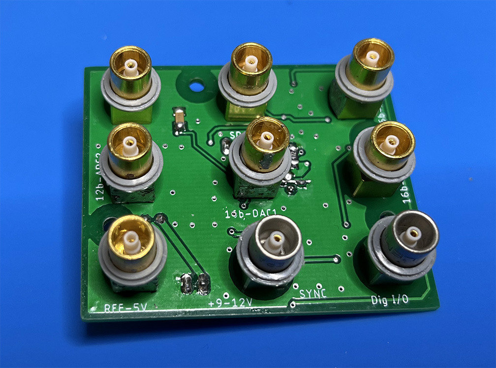
The ADS1115 on the Display, WLAN and IO driver board were a bit noisy. Moreover, an extra DAC for doing external measurements was missing. Thus I dedicated a separate Digital/Analog IO board that sits right behind the front panel with minimal wire lengths. It sports two 16bit ADC's based on MAX1169, two 12bit ADC based on MAX1236, one 16bit DAC based on MAX5217, plus a precision voltage reference MAX6350, with all IO protected and buffered by AD822. This is the final ingredient for reproducing the full functionality of my old desktop system, albeit now with much better technical specs.
Here are the schematics:
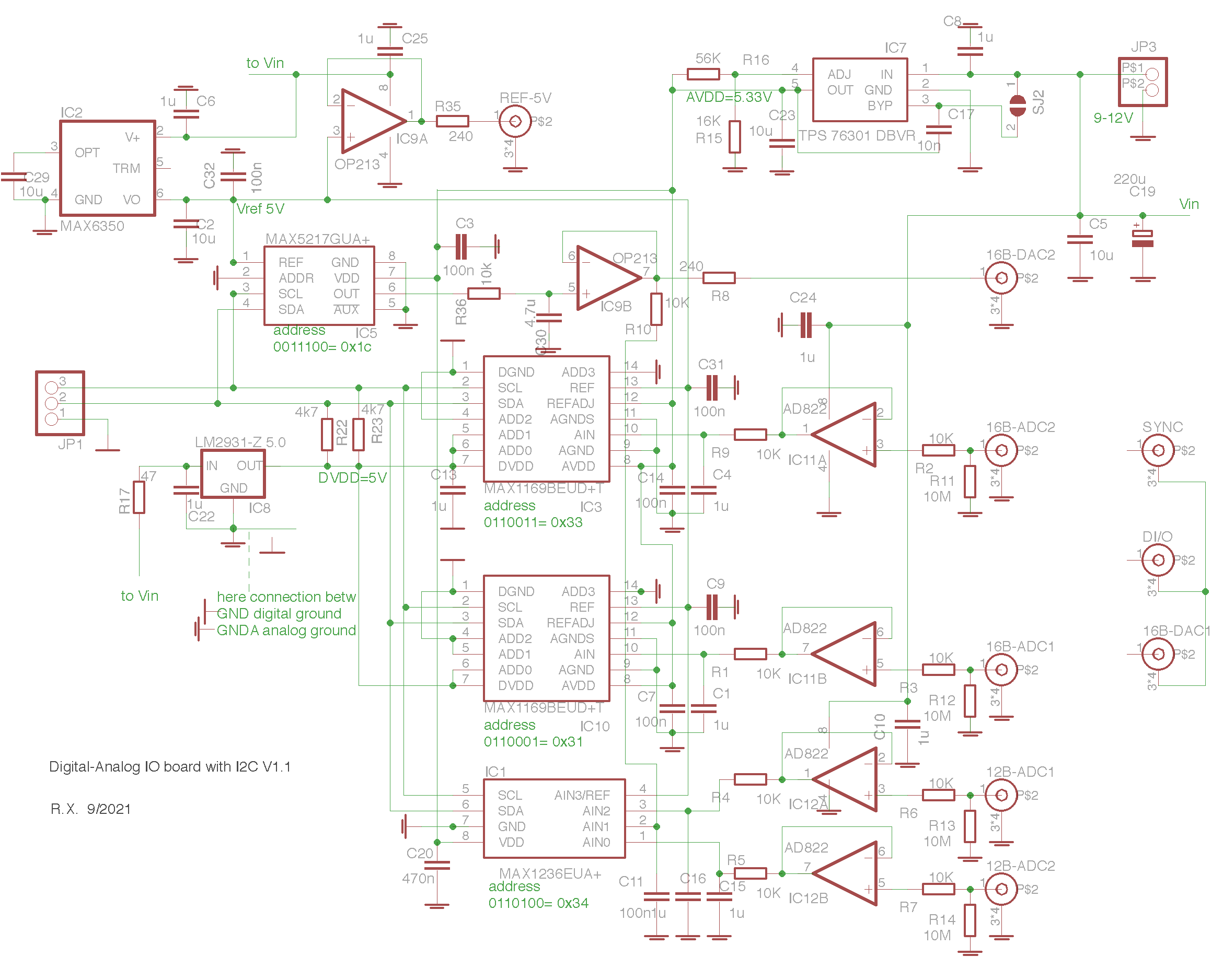
Some connectors just go through and are to be connected to the laser driver board (another 16 bit DAC output) and to the TFT-interface ESP32 board (sync signal and general purpose IO), also the I2C bus is connected to the ESP32 via a level shifter.
For the PWM controller, see here.
Here are some preliminary measurements of the LD driver output, I may present more in the future.
As said, one of the design goals, besides stability, was to keep the noise down despite of digital control. So naturally I started with noise measurements, which were done using the amplifiers and setup described here. The measurements were done with a 5Ohm dummy load in lieu of the laser diode. As with all low-noise measurements, a proper setup is critical: extremely careful cabling in- and outside, no ground loops, mains isolation transformer for the whole desktop device, battery operated amplifiers, no LED lights nearby, avoiding even the slightest cable movements, etc.
The major concerns were digital feedthrough from the I2C bus via the DAC, plus the coupling of the PWM signal from the TEC controller. The former could be eliminated by blanking an I2C isolator, ie, making briefly contact to the bus only while the DAC setting is being changed. This is explained above. How effective this is can be seen here where the connection to the I2C bus was switched off only in the second half of the picture:
![]()
This measurement was done with my 0.1-10Hz low noise amplifier plus isolation amplifier with total gain 10^5; thus the vertical setting of 100mV/div corresponds to 1uV/div, horizontal 1s/div. In the best of all setups, about 1.2uV/pp could be achieved, which translates to 0.24uA/pp for the current through the 5Ohm load (for 0.1-10Hz, at 400mA):
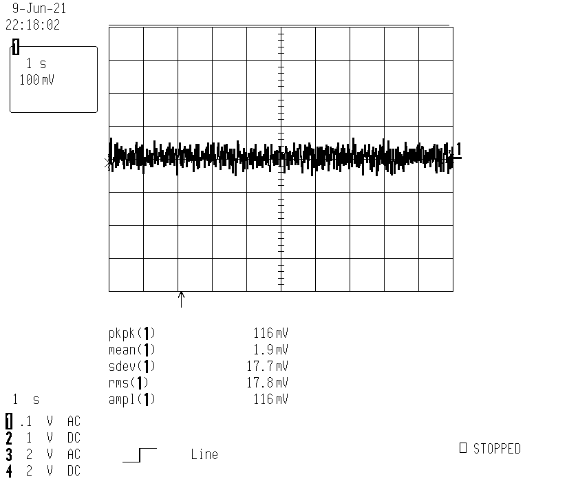
This is as good as the voltage reference can do; the OP213 opamp contributes just about 1/10th of that.
More of a concern is the 60khz PWM signal from the TEC controller, arising from large switched currents, and there is little hope to eliminate it completely. Especially if the TEC current runs together with the diode current alongside in the same cable to the laser head. For this purpose I added two extra 1mH 3A chokes plus filter capacitors to the bi-directional PWM output, which improved things a bit but not too much. When doing highly sensitive applications, one should run the signals with separate shielded cables to the laser head; I have put extra connectors to the front panel for this purpose. One should also add an extra LC low pass directly next to the laser diode. The following shows the imprint of the PWM signal on the diode current across the 5Ohm dummy load (using a separate cable for the TEC element):
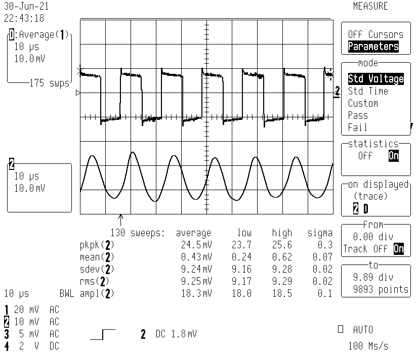
This measurement was done with my 0.1-100khz low noise amplifier with a gain of 10^4. Other noise was eliminated by averaging over the signal while triggering to the switching waveform (upper trace). From the lower trace we see a signal of about 2uV/pp at 60khz, which translates to 0.4uA/pp through the 5Ohm load. This signal is comparable to the total noise output and can't be can be recognized by the naked eye in the waveform otherwise.
Rather, the PWM signal figures pronouncedly in the power spectrum, ie, in the Fourier transform. The following shows the output spectrum from 0 to 100Khz for diode current off (lower trace) and 400mA (upper trace):
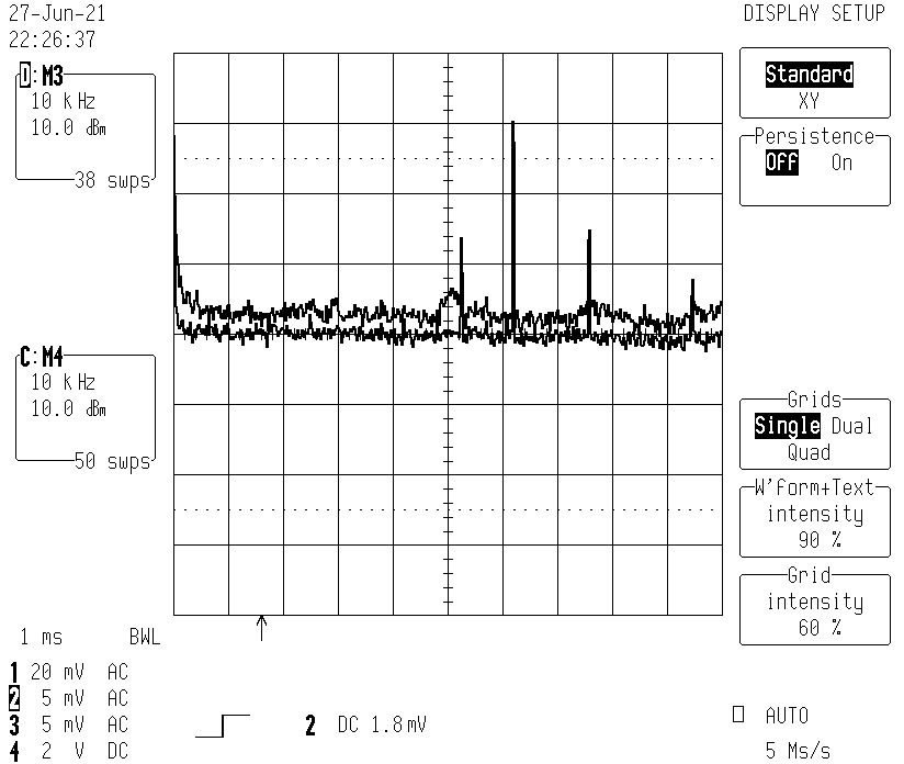
We see that the PWM signal is pretty much independent from the diode driver being on or off, which means that it rather must come from direct coupling into the wires and not via the driver. Likely a watertight RF-style shielding of the PCBs would improve on that. On the other hand, the general broadband noise level is elevated by about 5dB when the driver is switched on. So this component of the noise is due to the driver. The curves above refer to a TEC current of 200mA, which corresponds to typical operation.
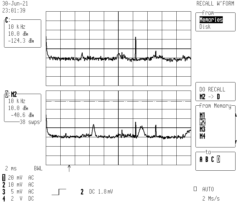
In the plots below, the upper trace corresponds to a TEC current of said 200mA, while the lower one to 1.5A. Clearly the integrated noise is higher while the 60khz peak is more spread out:
Now some stability measurements of diode current, temperature and TEC current for the whole integrated system, when driving a laser head with temperature stabilized diode mount (which will be the main application of the driver). The blue curves reflect data from the digital power supply under consideration, exported via WLAN to LabVIEW. The orange curves stem from external 5- and 6-digit DMMs as independent cross checks; for the temperature, a second independent thermistor was used. Only relative temperatures are shown, the absolute temperatures cannot be measured as accurately, of course.
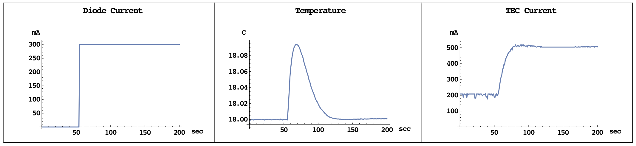
The first plots show effect of switching on the diode:
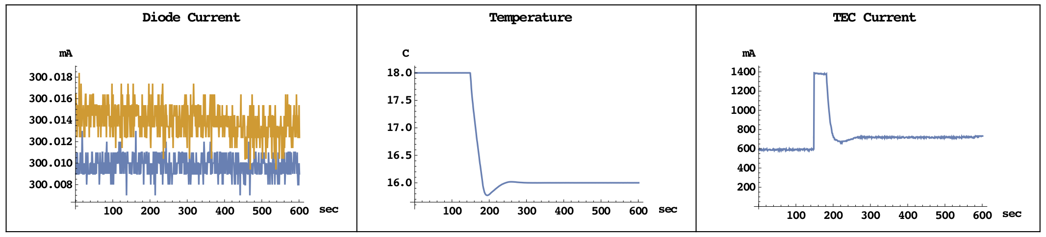
Now the temperature was changed. The diode current is unaffected, while the TEC current response is precisely as expected:
Here stability for about 12 hours under almost constant operating conditions:
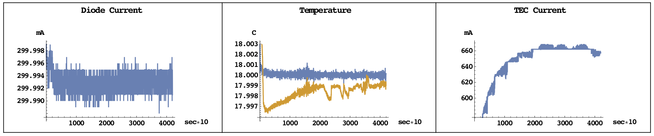
Unsurprisingly the internal data don't show any drift, as the voltages from the DACs and the ADC's derive from the same voltage reference. This is why a comparison with independent DMMs is important. The temperature excursions from the DMM came form me entering the room, while the laser head wasn't well shielded. The plateaus in the TEC current stem are artifacts from naive averaging.
Here a comparison of noise and resolution of 3 different data channels for 200mA laser current:
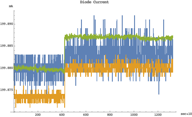
The current step corresponds to an increase of 8uA, which is the minimum stepsize of the 16-bit DAC MAX5217.
Green: external Rigol 3068 DMM: obviously best
Orange: 16-bit MAX1169 ADC: about 2uV noise. This is the monitor output of the circuit described above, with great care taken about noise - isolated low noise supply, separate analog/digital grounds, low noise reference. The resolution is better than 8uA due to averaging and oversampling in software.
Blue: internal 16-bit ADS1115: The ADC is located on the display driver board without further isolation and runs off the digitally polluted 5V power; uses internal voltage reference. Despite averaging and oversampling in software the resolution is much worse due to noise.
Upshot is that a proper circuit design and layout is crucial in order to get anywhere close to good resolution. On top of that, the quality of both ADC's appears quite different too.
Finally, here pics of LabVIEW interfaces that allow for remote control. The first picture shows the frontend for scanning over diode current and temperature:
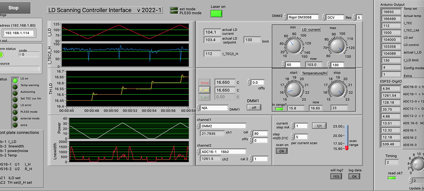
More details are given here.
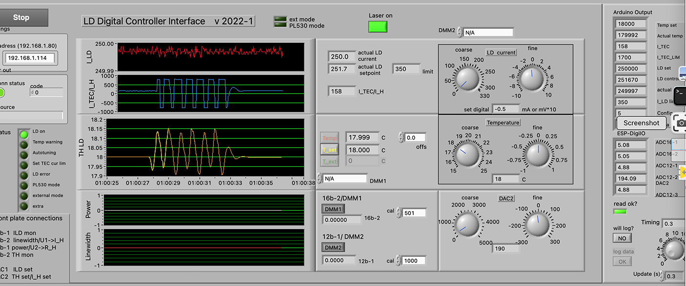
The second picture shows the effect PID-autotuning: the blue trace shows the test signal (TEC current), and the yellow trace shows the response signal (LD temperature). From these data suitable parameters for the PID control loop are automatically computed and stored under the currently selected operating profile. The software implementation is explained on the page of my Arduino-TEC controller.
Lots of code for both the Arduino Mega and the ESP32 still needs further debugging and cleaning up.
Current: Vers. 1.0 - May 2023
Return to home page